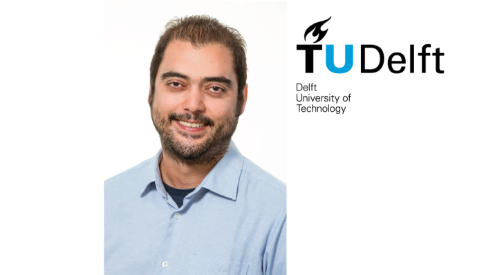
I am working at Photovoltaic Materials and Devices (PVMD) group in TU Delft, the Netherlands since 2021, with my main interest in plasma processing, and of course its applications on photovoltaics. I completed my PhD in 2015, focusing on optimization of vacuum systems, plasma processes and layer developments used in silicon solar cells’ manufacturing. At SiLEAN, I am busy with plasma based nano-texturing processes and coordinating the experimental activities of TU Delft.
What was your original motivation to become a researcher?
I believe I was deeply impressed by sci-fi books (by Robert A. Heinlein, Arthur C. Clarke, Philipp K. Dick and many more) that I read when I was a kid. Star Trek series was the cherry on the pie. I studied chemical engineering. When all of us graduated, most of my friends started working on solution based processes (I have to admit distillation has its own merits). On the other hand, I already made up my mind to work with vacuum systems and plasmas. It took me a couple of days to realize that I will not be able to go to space, so I decided to work for our own beloved planet’s sake. This is where PV popped up.
What is your (main) research area today?
My research area is to develop new processes (thanks mostly to plasma) for c-Si based solar cells such as improving layer properties, developing new layers, modulating the surfaces to enhance light trapping, and so on.
What is the main objective of your team in SiLEAN?
Team TUD works on several aspects in SiLEAN such as advanced texturing methods for Si wafers, development of transition metal oxides, reduction/elimination of Silver used in metallization processes and lastly a crucial topic, however a relatively late boomer: Research on environmental impact and circularity.
What expertise and facilities does your team have to meet those objectives?
We already demonstrated our nano-texturing skills in several papers and we hold the world record efficiency of 23.83% on MoOx based SHJ solar cells. We have EKL (Else Kooi Laboratory) and ESP (Electrical Sustainable Power Lab) laboratories for fabrication and characterization of PV devices. In these labs, not only PV researchers, but also experts from different research fields work together under one roof. This diversity yields in different point of views to approach the research topics and always provides us with creativity.
Which aspects of your research at SiLEAN do you believe are the most innovative and what unique opportunities offer SiLEAN to yourself and/or your organisation?
I believe the development of light trapping schemes, such as modulation of epi-wafers’ surfaces with the performance targeted in SiLEAN is the most innovative aspect of my particular research. Also, it is great to collaborate with industry partners (who can fabricate epi-wafers) and leading research institutions.
How do you see the future use of the SiLEAN results and the impact of SiLEAN project in our daily lives?
I hope the outcome of the SiLEAN project will help preventing monopolization of PV industry, considering the goals of low manufacturing costs and reduction of dependence on scarce/critical materials. Affordable and sustainable renewable energy, also accelerated energy transition is the only way to go for the future of our planet unless we want an uninhabitable environment.


