SiLEAN project
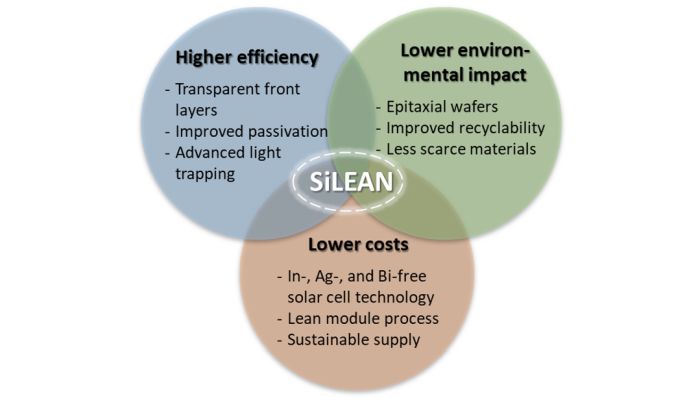
About SiLEAN
To meet the growing energy demand, reduce greenhouse gas emissions, and lower electricity costs, highly efficient and cost-effective photovoltaic (PV) technologies with low carbon footprints are essential.
SiLEAN is a 3-year project addressing key challenges such as the high energy and material requirements for Si wafer manufacturing, limited current generation, and the use of scarce materials like silver, bismuth, and indium.
In the project, a lean process chain will be developed for the next generation of silicon heterojunction (SHJ) solar cells. Our strategy involves utilizing epitaxially-grown wafers that require less energy, developing alternatives to the highly absorptive hydrogenated amorphous silicon for passivation and carrier-selective contacts, creating indium-free contact layers and silver-free metallization concepts, and implementing bismuth-free interconnection methods.
Our goal is to achieve solar cell efficiencies greater than 25.5% and module efficiencies over 23.5%, while reducing Si wafer and contacting costs by 50% and lowering the carbon footprint by up to 75%.
Objectives
Development of epitaxially grown ultra-thin epi-Si wafers from the gas phase with increased quality and advanced light management.
Development of transparent passivating contacts (TPCs) and Transition Metal Oxides (TMOs) for SHJ solar cells.
Demonstration of novel contacts for thin SHJ solar cells with a strong reduction of scarce materials.
Validation of SiLEAN solution and integration into mini modules, with high potential for high mass production.
Concept
The limitations in current SHJ solar modules hinder mass production on a terawatt scale. The SiLEAN project aims to introduce innovative approaches throughout the entire manufacturing chain to overcome these obstacles, developing and implementing lean processes that are fully compatible with industrial solar cell manufacturing lines.
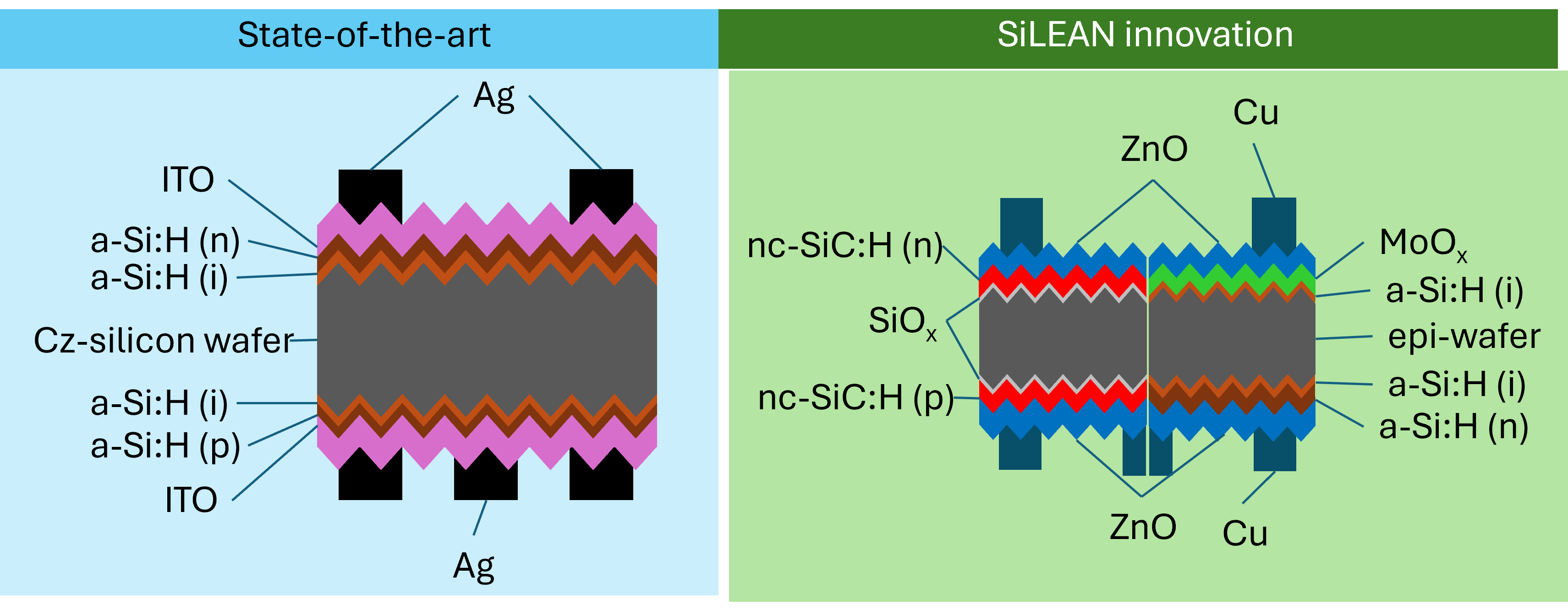
This includes replacing traditional silicon wafers with low-energy, material-efficient epitaxially-grown wafers to reduce costs and improve sustainability. To boost cell performance and reduce critical material usage, high-absorptive front layers are replaced with transparent, indium-free alternatives. In metallization, silver is substituted with copper and metal-free designs are being developed to lower manufacturing costs. Additionally, new multi-wire interconnection methods without bismuth are being created, integrating cell interconnection and encapsulation.
By addressing these key challenges, SiLEAN will enhance the sustainability of SHJ solar cells and modules, achieving higher efficiency and lower costs, ultimately enabling the upscaling of SHJ technology.
Approach
The SiLEAN project is developing several innovative solutions across the production chain to enhance SHJ solar technology:
- Wafer Manufacturing: Replacing traditional silicon wafers with energy and material efficient epitaxially-grown wafers, resulting in lower costs and better sustainability through reduced silicon consumption and CO2 footprint.
- Texturing: Implementing advanced surface texturing to minimize silicon loss and improve light management. This includes creating nanopyramids ≤ 1 μm and utilizing black silicon.
- Thin Film Deposition: Replacing high-absorptive front layers with more transparent, indium-free alternatives to enhance cell performance and reduce the use of critical materials.
- Metallization: Substituting silver metallization with copper and developing new designs for metal-free solar cell contacts, through copper plating, copper screen-printing, and carbon/graphene-based screen-printing, to lower manufacturing costs.
- Interconnection: Developing multi-wire interconnection methods without bismuth, integrating cell interconnection and encapsulation.
Mission
SiLEAN brings together a multi-disciplinary consortium with three research institutes, one university, four SMEs, and one industry partner located in 6 different countries including Germany, Belgium, the Netherlands, Italy, Switzerland, and Türkiye to develop advanced innovations in silicon heterojunction solar cell technology.
The novel SiLEAN solutions, featuring silver-less or silver-free metallization concepts, will mitigate high supply risks. By using alternative materials to those in standard SHJ cells—such as replacing Ag, In, and doped silicon—SiLEAN technology will benefit more industrial players across the value chain, from materials suppliers to equipment and module manufacturers.
Results
Si wafers with thickness < 100 µm and advanced light-management architecture for optimal efficiency trade-off.
Solar cell efficiency > 25.5% using ZnO-based TCOs and Ag-free metallization.
Design of innovative SHJ mini modules with energy-conversion efficiency >23.5% paving the way for terawatt-scale production.
A 50% reduction in manufacturing costs, making the process compatible with mass production.
Full life-cycle analysis to assess the reduction of the environmental impacts and ecological risks of industrialized modules based on the SiLEAN (In-, Ag-, and Bi-free) solar cell technology.
Facts and figures
Acronym: SiLEAN
Duration: 36 months
Start date: 1st May 2024
EC Funding: € 2,996,153.75
Publications
SiLEAN is conducting research in the field of PV technology and will disseminate scientific results to peers in the field through scientific publications. All relevant publications will be posted on this website.