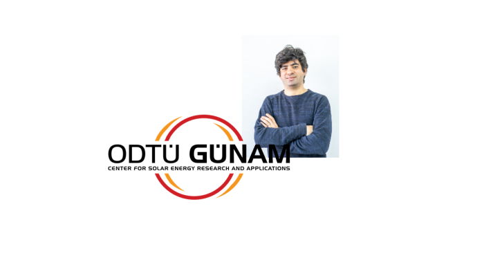
Hisham Nasser is currently working at ODTÜ-GÜNAM in Ankara, Turkey, with main expertise lies in the science and technology of photovoltaics. He completed his PhD in 2015, focusing on light trapping in silicon solar cells. Since 2021, he has been leading a team dedicated to developing efficient passivated contact-based silicon solar cells and bottom cells for silicon/perovskite tandem structures. At SiLEAN, he will be leading the activities of ODTÜ-GÜNAM to develop In-free TCO and upscale the process and to develop nanotexturing processes focusing on industrial feasibility.
What was your original motivation to become a researcher?
My original motivation to become a researcher stemmed from a deep curiosity about how things work, combined with a strong commitment to addressing significant challenges—particularly those related to sustainable and eco-designed energy solutions.
What is your (main) research area today?
Passivated contact-based silicon solar cells (TOPCon & SHJ), selective and transparent contacts, Si bottom cells for silicon/perovskite tandem solar cells, light trapping for solar cells.
What is the main objective of your team in SiLEAN?
At SiLEAN, the team is working on the development of indium-free transparent conductive oxides (TCOs) and scaling up processes for large wafer formats (≥ M10), as well as advancing light-trapping nano-texturing techniques for thin silicon with high throughput.
What expertise and facilities does your team have to meet those objectives?
Our team at SiLEAN brings together a unique combination of expertise and state-of-the-art facilities, enabling us to successfully achieve our ambitious goals of developing In-free TCOs and advancing light-trapping nano-texturing processes. With over 10 years of experience in TCO development for Silicon Heterojunction (SHJ) and selective contact solar cells, we have built a strong foundation in these materials. Light-trapping processes have been a central focus of our research, particularly for SHJ and various silicon cell architectures.
Our specialized facilities include high-throughput, industrial-grade tools, such as wet benches, atomic layer deposition (ALD), and reactive ion etching (RIE), all designed to meet the rigorous demands of large-scale production. Additionally, we have access to cutting-edge characterization equipment for structural, morphological, electrical, and optical analysis, ensuring precise and comprehensive evaluation of layers, surfaces, and associated processes.
Which aspects of your research at SiLEAN do you believe are the most innovative and what unique opportunities offer SiLEAN to yourself and/or your organisation?My research at SiLEAN focuses on developing materials and layers for cost-effective and eco-desgined silicon photovoltaics using innovative and industry ready approaches. I meet and discuss current and future PV technologies with inspiring people, it couldn’t be better.
How do you see the future use of the SiLEAN results and the impact of SiLEAN project in our daily lives?
I see the future use of SiLEAN’s results as transformative for both the renewable energy industry and society as a whole. The innovative materials and technologies to be developed in SiLEAN will play a key role in making solar power more effective, scalable, and affordable. This can lead to widespread adoption of renewable energy, both for individual consumers and large-scale infrastructure projects. Ultimately, SiLEAN’s work will help us move towards a more sustainable, energy-independent future, contributing to both environmental protection and economic growth posively impacting daily lives.


