SiLEAN achieves high-performance Indium-Free Transparent Conductive Oxide
The SiLEAN project has reached an important milestone in its mission to reduce the use of critical raw materials in photovoltaic manufacturing. As part of this effort, the consortium has successfully demonstrated a high-performance indium-free Transparent Conductive Oxide (TCO) layer with excellent optical and electrical properties.
This achievement focuses on the development of hydrogenated aluminium-doped zinc oxide (AZO:H) using spatial atomic layer deposition (sALD)—a technique well suited for industrial-scale production due to its ability to deliver uniform, high-quality coatings over large areas. By carefully optimizing the deposition process, including the use of tailored precursor combinations and controlled doping conditions, the team produced AZO:H layers with a thickness of around 83 nm that meet the stringent requirements of ultra-thin silicon heterojunction (SHJ) solar cells.
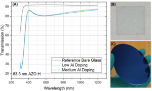
The figure below illustrates the optical performance of the optimized 83.3 nm AZO:H layer.
The optimized films demonstrate optical transmission above 80% across a broad spectral range (380–1200 nm), making them highly suitable for use in high-efficiency devices. At the same time, the layers achieve competitive electrical performance, with sheet resistance values as low as 3.5 kΩ/sq.
The study also provided valuable insight into the material’s behaviour. It was found that excessive aluminium doping can lead to the formation of inactive clusters, limiting performance. By reducing the doping level, the team improved both transparency and conductivity—an important step toward further optimization.
Building on these findings, the project is now exploring advanced deposition strategies, including so-called “supercycle” approaches, to further fine-tune material properties and enhance device performance.
This result represents a significant step toward indium-free, scalable, and high-efficiency solar cell technologies, reinforcing SiLEAN’s contribution to a more sustainable and resource-efficient photovoltaic value chain.