
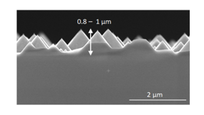
Within the SiLEAN project, random nanopyramid textures for NexWafe’s kerfless silicon EpiWafers are developed to support high-efficiency silicon heterojunction solar cells on thinner, more sustainable wafers. Reducing wafer thickness requires improved light management while minimizing performance losses.
The nanopyramids are fabricated using an industry-compatible alkaline wet-etching process. By optimizing additives and process parameters, pyramid heights below 1 μm were achieved while consuming less than 5 μm of silicon, making the approach particularly suitable for ultra-thin wafers.
The process was successfully demonstrated on both conventional Czochralski silicon wafers and NexWafe EpiWafers, below 100 micron thickness. Optical, morphological, and electrical characterization showed that EpiWafers develop similar texture morphologies, reflectance, and passivation quality as conventional wafers, confirming compatibility with industrial texturing processes. The next stage for the last year of the project will be to transfer this process to an-line texturing wetbench.
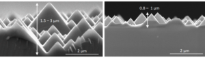
Standard random micro-pyramids |
SiLEAN nano-pyramids on EpiWafer |